
In the realm of semiconductor manufacturing and advanced material research, thin film deposition techniques play a pivotal role in creating the intricate structures that power modern electronics. Among the arsenal of methods available, the utilization of tungsten boats has emerged as a cornerstone in achieving precise and uniform thin film coatings.
Tungsten boats, characterized by their high melting point and excellent thermal conductivity, are indispensable tools in vacuum evaporation processes for depositing thin films onto substrates. This technique, known as physical vapor deposition (PVD), involves the vaporization of a solid material within a vacuum environment, followed by its condensation onto a substrate to form a thin film.
One of the primary applications of tungsten boats is in thermal evaporation, where materials such as metals, oxides, and semiconductors are heated to their vaporization point within the boat crucible. As the material evaporates, it condenses onto the substrate, resulting in a thin film with controlled thickness and composition. This process is crucial in the fabrication of semiconductor devices, optical coatings, and surface modifications for various industrial and scientific applications.
The unique properties of tungsten, including its high melting point of 3422°C and minimal reactivity with most materials at elevated temperatures, make it an ideal choice for use in evaporation boats. Unlike other materials, tungsten boats exhibit exceptional stability and durability, ensuring consistent performance even under extreme operating conditions.
In semiconductor manufacturing, the demand for precise and uniform thin film coatings continues to grow with the advancement of electronic devices. Tungsten boats have become indispensable tools in this field, enabling the deposition of thin films with high purity and uniformity, essential for the fabrication of integrated circuits and other semiconductor components.
Furthermore, tungsten boats find applications beyond semiconductor manufacturing, playing a vital role in research areas such as electron microscopy, metallurgy, and surface science. Researchers rely on the versatility and reliability of tungsten boats to explore new materials and develop innovative thin film technologies.
As the semiconductor industry pushes the boundaries of miniaturization and functionality, the importance of thin film deposition techniques, particularly those utilizing tungsten boats, will continue to rise. With ongoing advancements in material science and manufacturing processes, tungsten boats are poised to remain at the forefront of thin film deposition, driving innovation in electronics and beyond.
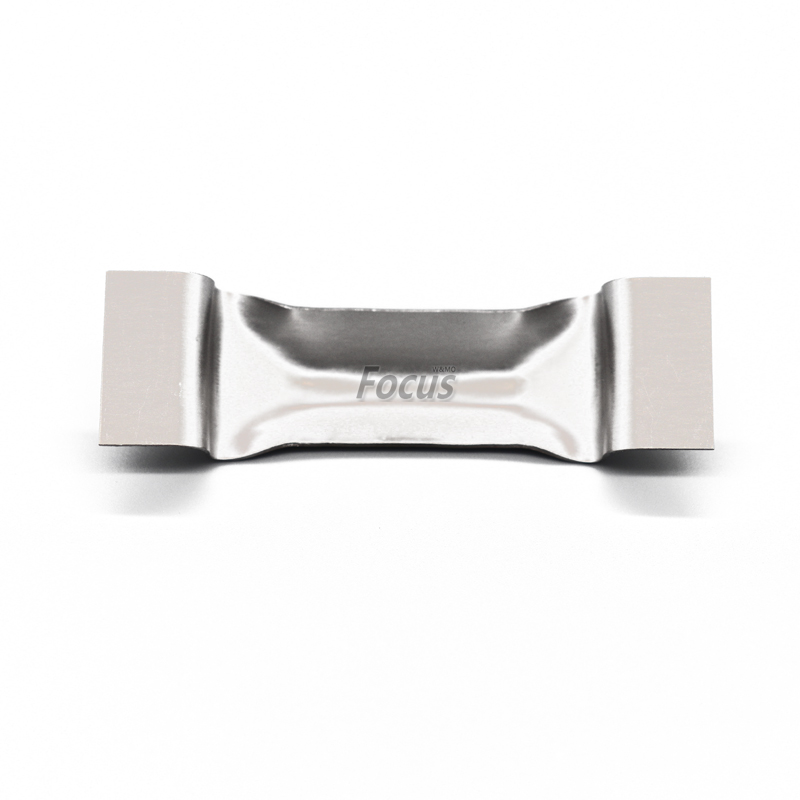
Our tungsten boat has all kinds of model which contains:210, 215, 216, 308, 310, 312, 313, 315, 316, 318, 514, 515. And special size could be customized according to your drawings or requirements. If you want to learn more about tungsten boat, pls click “tungsten boat“.
